Wednesday, August 13, 2008

LIST OF EXPERIMENTS

1. SERIES AND PARALLEL LCR CIRCUITS
2.. I-V CHARACTERISTICS OF A ZENER DIODE
3. CHARACTERISTICS OF A TRANSISTOR
4. BAND GAP OF A SEMICONDUCTOR
5. ULTRASONIC INTERFEROMETER (MEASUREMENT OF VELOCITY OF SOUND IN SOLIDS AND LIQUIDS)
6. DIELECTRIC CONSTANT (MEASUREMENT OF DIELECTRIC CONSTANT)
7. MAGNETIC PROPERTIES (B-H GRAPH METHOD)
8. DIFFRACTION (MEASUREMENT OF WAVELENGTH OF LASER/Hg SOURCE USING DIFFRACTION GRATING)
9. PLANCK’S CONSTANT (DETERMINATION OF PLANCK’S CONSTANT USING LED OR USING THE PRINCIPLE OF PHOTOELECTRIC EFFECT)
10. ELECTRICAL RESISTIVITY (FOUR PROBE METHOD)
11. VERIFICATION OF STEFAN’S LAW
12. DETERMINATION OF FERMI ENERGY

1.SERIES AND PARALLEL LCR CIRCUITS

AIM: to study the frequency response of the series and parallel LCR circuits and hence to determine 1) the resonant frequency,
2) the quality factor,
3) bandwidth of the circuit and
4) the self inductance of the given inductor.
APPARATUS: Audio frequency oscillator, ac milliammeter, resistor, capacitor and inductor.
PRINCIPLE: When a capacitance C, inductance L and resistance R are connected in series with an ac source, it forms a series resonance circuit. The impedance of a series resonance circuit is given by,
Z =Ö R2+(wL-1/wc)2 where w=2pf; f is the frequency of ac. When inductive reactance is equal to capacitive reactance (wL=1/wc), frequency of the applied emf is equal to the natural frequency of the LCR circuit. This is called resonance.
\At resonance, wL=1/wc
w2=1/LC
(2pf0)2=1/LC
f0=1/2pÖLC
f0 is called resonant frequency. At resonant frequency, current in the circuit is maximum.
The value of the inductor, L=1/4p2f02c
Quality factor Q=1/RÖL/C
From frequency response graph, Q=f0/b whereb=fb-fa is the bandwidth.
In a parallel resonant circuit, an ac source is connected across a parallel combination of an inductance L and capacitance C. Let R be the resistance in the inductance branch. Here, at resonance, the current is minimum.
PROCEDURE:
1) Series resonant circuit
The circuit connections are made as shown in figure 1. The oscillator is switched on and the output of the oscillator is adjusted to a maximum value which is kept constant throughout the experiment. The frequency is increased in steps and corresponding reading of the current (I) in mA is recorded. Care should be taken to locate resonant frequency (frequency corresponding to maximum current) with maximum accuracy. The graph of circuit current as a function of frequency is plotted (figure 2).
The value of inductance L is verified using the formula L= 1/4p2f02c
A straight line drawn parallel to frequency axis at the point Imax/Ö2 on the Y-axis, cuts the curve at two points corresponds to the frequencies fa and fb on the X-axis.
Q-factor is evaluated from the graph, Q=f0/ fb-fa
The theoretical value of the Q-factor is evaluated using the formula
Q=1/RÖL/C
2) Parallel resonant circuit
The circuit connections are made as shown in figure (3). The oscillator is switched on and the output of the oscillator is adjusted to a maximum value which is kept constant throughout the experiment. The frequency is increased in steps and corresponding reading of the current (I) in mA is recorded. Care should be taken to locate resonant frequency (frequency corresponding to minimum current) with maximum accuracy. The graph of circuit current as a function of frequency is plotted (figure 4).
The value of inductance L is verified using the formula L= 1/4p2f02c
A straight line drawn parallel to frequency axis at the point Imin/Ö2 on the Y-axis, cuts the curve at two points corresponds to the frequencies fa and fb on the X-axis.
Q-factor is evaluated from the graph, Q=f0/ fb-fa
The theoretical value of the Q-factor is evaluated using the formula
Q=1/RÖL/C


CALCULATIONS:
1) Series resonant circuit
Resonant frequency f0 =
Inductance L=1/4p2f02c=
From graph, fa = fb=
Bandwidth Df = fb-fa=
Quality factor Q = f0/Df=
Theoretical value Q=1/RÖL/C=
2) Parallel resonant circuit
Resonant frequency f0 =
Inductance L=1/4p2f02c=
From graph, fa = fb=
Bandwidth Df = fb-fa=
Quality factor Q = f0/Df=
Theoretical value Q=1/RÖL/C=
RESULTS:
1) Series resonant circuit
Resonant frequency (a) theoretically =
(b) graphically =
Inductance, L (theoretically) =
Bandwidth =
Q-factor (a) theoretically =
(b) graphically =
2) Parallel resonant circuit
Resonant frequency (a) theoretically =
(b) graphically =
Inductance, L (theoretically) =
Bandwidth =
Q-factor (a) theoretically =
(b) graphically =

I-V CHARACTERISTICS OF A ZENER DIODE

AIM: To draw the V-I characteristics of a given Zener diode and to determine the reverse breakdown voltage forward knee voltage and Zener resistance.
APPARATUS: Zener diode, 1KW resistor, DC regulated power supply, voltmeter, milliammeter.
PRINCIPLE: A Zener diode is essentially a heavily doped p-n junction diode. Its symbol is shown in figure (1).
When the Zener diode is forward biased, the forward current increases with the increase in applied voltage. When it is reverse biased, a small reverse current flows until the breakdown voltage is reached. In the vicinity of breakdown region, the reverse current starts rising rapidly because of avalanche effect. Finally a sharp increase in current occurs when the Zener breakdown voltage (Vz) is reached. In this region, a small voltage change results in a large current change. This voltage limiting characteristics of a Zener diode makes it a good voltage regulator.
PROCEDURE:
FORWARD CHARACTERISTICS:
Connections are made as shown in figure (2).
The voltage is varied gradually and the corresponding current values are noted down.
REVERSE CHARACTERISTICS:
Connections are made as shown in figure (3).
The voltage is varied gradually and the corresponding current values are noted down.
A graph can be plotted with the voltage along X-axis and the current along the Y-axis. During the forward bias, the voltage at which current increases sharply is called forward knee voltage (Vk). In the reverse bias graph, extrapolating straight line portion to the X-axis will yield Zener breakdown voltage. The slope on the linear part of the curve gives Zener resistance, Rz = DV/DI


OBSERVATIONS:
FORWARD CHARACTERISTICS:
Voltage ( Volts) Current (mA)
REVERSE CHARACTERISTICS:
Voltage ( Volts) Current (mA)


CALCULATIONS:
From I-V characteristics graph,
DV =
DI =
\RZ = DV/DI =
RESULTS:
I-V characteristics of a Zener diode are drawn.
The forward knee voltage (Vk) = Volts.
The Zener breakdown voltage (Vz) = Volts.
The Zener resistance (Rz) = Ohms

3.Transistor-Characteristics

AIM: To draw the input and output characteristics of given N-P-N transistor in the Common Emitter configuration and hence to determine the input resistance, output resistance and current gain b.
APPARATUS: N-P-N transistor, Variable DC power supplies, Digital voltmeter, DC Microammeter, DC Milliammeter, 100 KW Resistor and 100W Resistor.
PRINCIPLE: Transistor is a three terminal, two junction semiconductor device. The three terminals are Emitter, Base and Collector. In an N-P-N transistor, a P-type semiconductor is sandwiched between two N-type materials. Here Emitter is heavily doped, the Base is lightly doped and the Collector is intermediately doped. Common Emitter configuration is most effective because of its high current gain, high voltage and power gain. In Common Emitter configuration, Emitter terminal is made common to both input and output circuits. Input junction (Base-Emitter) is forward biased and output junction (Collector-Emitter) is reverse biased so that the input junction is having low resistance (since it is forward biased) and output junction high resistance (since it is reverse biased).
Input characteristics of a transistor is a curve showing the variation of input (Base) current IB as a function of input (Base-Emitter) voltage VBE, when the output (Collector-Emitter) voltage VCE is kept constant.
Input resistance Ri = (DVBE/ DIB)
Output characteristics of a transistor is a curve showing variations of output current IC as a function of output voltage VCE, when the input current IB is kept constant.
Output resistance Ro = DVCE/DIC
Current gain b = DIC/DIB
PROCEDURE: The circuit connections are made as shown in figure.

(a) Input characteristics: Power supply VCC is switched on and VCE is adjusted to a desired value by varying VCC. Base-Emitter voltage (VBE) is varied and corresponding base current (IB) is noted down. The readings are plotted with VBE along X-axis and IB along Y-axis. Slope of the graph will input resistance.
(b) Output characteristics: By varying VBB, IB is adjusted to a desired value. Now VCE is is varied and corresponding value of IC is noted down. The readings are plotted with VCE along X-axis and IC along Y-axis. Another set of observation is taken for different IB value and the graph is plotted. Slope of the graph will give output resistance.
(c) Current gain: Keeping VCE constant, collector current IC is noted for different values of base current IB. The experiment is repeated for various constant values of VCE and readings are tabulated. A graph is drawn with IB along X-axis and IC along Y-axis. Slope of the graph will give current gain b.

OBERVATIONS:
(a) Input characteristics:
VCE =
VBE IB


(b) Output characteristics:
IB IB IB
VCE IC VCE IC VCE IC

(c) Current gain:
VCE VCE VCE
IB IC IB IC IBIC

CALCULATIONS:
(1) Slope of the DVBE - DIB graph (Input resistance Ri) = DVBE/ DIB =
(2) Slope of the DVCE - DIC graph (Output resistance Ro) = DVCE/ DIC =
(3) Slope of the DIB - DIC graph (Current gain b) = DIB/ DIC =
RESULTS:
(1) The input and output characteristics are drawn.
(2) Input resistance Ri =
(3) Output resistance Ro =
(4) Current gain b
=

BAND GAP OF A SEMICONDUCTOR

AIM: To determine the forbidden energy gap of a semiconductor.
APPARATUS: P-N diode, DC regulated power supply, Voltmeter, Milliammeter, 1 KW resistor, Beaker, Thermometer, Heater.
PRINCIPLE: The forbidden energy gap of a material is a collection of energy levels above the top of the valence band and below the bottom of the conduction band. For the determination of the energy gap of a semiconductor, a semiconductor in the form of P-N diode is used. The forward current in such a diode is given by,
If = Is[exp(eV/hkBT)-1]
Where V = forward voltage across the junction, e = electronic charge, kB = Boltzmann constant, T = absolute temperature, Is = reverse saturation constant and h = a constant called emission co-efficient.
Is is given by,
Is = BT3ex(Eg/kBT) where B is a constant.
For a low constant forward current, the above equations can be approximated to yield an equation,
eV = Eg - hkBT
Hence a plot of V versus T gives a straight line with the V-intercept equal to Eg/e at T=0K. From this, the energy gap of the semiconductor can be obtained.
PROCEDURE: The circuit is built up as shown in figure (1). The forward biased voltage is kept at room temperature. A constant forward current is passed through the diode and the voltage developed across the diode at this temperature is noted. Then the diode is immersed in hot water bath. Voltage across the diode is noted down for different temperatures as water bath cools down. The readings are noted down till the water bath attains room temperature.
A graph with voltage along Y-axis and temperature along X-axis is drawn. The Y-intercept of the graph at 0K is found. From this the energy gap of the semiconductor is calculated.
OBSERVATIONS:
Constant forward current through the diode =
Temperature ( 0C ) Temperature ( K ) Junction Voltage (V)

CALCULATION:
Y-intercept of the graph (Eg/e) =
\Eg =
RESULT: Energy gap of the given semiconductor =

5.ULTRASONIC INTERFEROMETER (MEASUREMENT OF VELOCITY OF SOUND IN SOLIDS AND LIQUIDS)

AIM: To find the velocity of sound in the given liquid using ultrasonic interferometer.
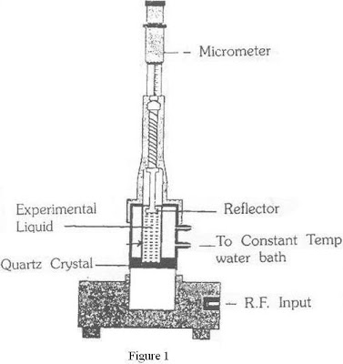
APPARATUS: ultrasonic interferometer (High frequency generator and measuring cell with micrometer and quartz crystal), Experimental liquid.
PRINCIPLE: An ultrasonic interferometer is a simple and direct device to determine the ultrasonic velocity in liquids with a high degree of accuracy. The principle employed in the measurement of velocity (v) is based on the accurate determination of the wavelength (l) in the medium. Ultrasonic waves of known frequency (f) are produced by a quartz crystal fixed at the bottom of the cell. These waves are reflected by a movable metallic plate kept parallel to the quartz crystal. If the separation between these two plates is exactly a whole acoustic resonance gives rise to an electrical reaction on the generator driving the quartz crystal and the anode current of the generator becomes a maximum.
If the distance is now increased or decreased and the variation is exactly l/2 or multiple of it, anode current becomes maximum. Using the value of l, the velocity (v) can be obtained by the relation
v = l × f
PROCEDURE: Unscrew the knurled cap of the cell and lift it away from double walled construction of the cell. In the middle portion of it pour experimental liquid and screw the knurled cap. Wipe out excess liquid overflowing from the cell. Insert the cell in the socket and clamp it with the help of a screw provided on its side. High frequency generator is connected to the cell using co-axial cables. Move the micrometer slowly in either clockwise or anticlockwise direction till the anode current on the ammeter on the high frequency generator shows a maximum or a minimum. Note the readings of micrometer. Take readings of a few consecutive maximum or minimum. The difference between two consecutive readings will give l/2. Once the wavelength (l) is known the velocity of ultrasonic wave in the liquid can be calculated.


OBSERVATIONS:
To find the least count of the micrometer
Number of rotations given to the screw head (N) =
Distance covered on the pitch scale (S) =
Pitch of the screw = S/N =
Total head scale divisions =
Least count (LC) = Pitch of the screw / Total head scale divisions =
Total reading (TR) = PSR + (HSD × LC)
Order of the maximum current
Micrometer reading(R1) mm
Order of the maximum current
Micrometer reading(R2) mm
Mean l =
CALCULATIONS:
Frequency of the ultrasonic wave (f) =
Wavelength of the ultrasonic wave (l) =
Velocity of the ultrasonic waves in the given liquid (v) = l × f
RESULT:
Velocity of the ultrasonic waves in the given liquid

6.Measurement of dielectric constant

AIM: To determine the dielectric constant of the dielectric medium present in a parallel plate capacitor.
APPARATUS: DC Regulated power supply, Electrolytic capacitor, Resistor, Digital voltmeter, Digital timer, Double plug key.
PRINCIPLE: Capacitors are devices which store electric energy by means of an electrostatic field and release this energy later. The voltage across the capacitor when it gets charged gradually at any instant of time t, is given by
Vc = V (1-e-t/RC),
where V is the voltage applied, R is the resistance and C the capacitance in the circuit. While discharging through the resistor R, the capacitor voltage at any instant t is given by,
Vc = V e-t/RC
Let T1/2 be the time required to charge or discharge a capacitor to 50%.
\When t= T1/2, Vc = V/2
V/2 = V e-t/RC
et/RC = 2
t/RC = loge 2 = 0.693
C = T1/2 /0.693 R
But C = Ke0A/d where A and d are the thickness and area of the dielectric material. e0 is the permittivity of free space and K the dielectric constant.
\K = d T1/2 /0.693e0AR
PROCEDURE: The circuit connections are made as shown in figure.
To begin with, the toggle key H is connected to point 1. Now the capacitor begins to get charged to higher voltage. The voltage across the capacitor is taken at every 10 seconds interval from the 0th second until capacitor voltage becomes practically constant. Now the capacitor is fully charged.
Now the toggle key H is connected to point 2. The voltage across the capacitor is taken at every 10 seconds interval from the 0th second until capacitor voltage becomes practically zero.
A graph is plotted with time T taken along X-axis and the capacitor voltage V along Y-axis. The charging mode curve and the discharging mode curve intersect at the point P. By referring the position ‘P’ to the time axis, the value of its abscissa T1/2 in seconds is found out. Now the dielectric constant K can be calculated.

OBSERVATIONS:
R=
Length L=
Breadth b=
Thichness d=
Area A= L × b=
Time (s) Voltage during charging (V) Voltage during discharging (V)

CALCULATIONS:
K = d T1/2 /0.693e0AR=
RESULT: The dielectric constant of the material in the given capacitor =

Monday, August 11, 2008

Experiment No.7

7

Experiment No.8

8

9.Determination of Planck's constant

AIM: To determine the value of Planck’s constant ‘h’ by a photocell.
APPARATUS: Photo emissive cell mounted in a box provided with a wide slit. Regulated DC power supply, Set of filters, Light source, Digital voltmeter and Digital microammeter.
PRINCIPLE: Planck’s constant ‘h’ is given by,
h = eVl/c where ‘e’ is the electron charge, ‘V’ the stopping potential corresponding to a light of wavelength ‘l’ and ‘c’ the velocity of light.
PROCEDURE: Connections are made as shown in figure (1). Light from the light source is allowed to fall on the photo cell which is enclosed in a box. The distance between the photocell and light source is adjusted such that there is sufficient flow of current. Now a suitable filter of known wavelength l1 is placed in the path of the light. A reading corresponding to the zero anode potential is observed in the microammeter. A small negative potential is applied which is gradually increased in small steps till the microammeter reading comes to zero. This is stopping potential V1 corresponding to the wavelength l1. Planck’s constant can be calculated using l1 and V1.The experiment is repeated with other filters and corresponding stopping potentials are noted. Planck’s constant is calculated in each case and mean value is taken.
OBSERVATIONS:
Wavelength (l) Stopping potential (V) Planck’s constant h = eVl/c
Mean value of h =
RESULT: Planck’s constant =

Experiment No.10

10

VERIFICATION OF STEFAN’S LAW

AIM: To verify Stefan’s law of radiation.
APPARATUS: DC Regulated power supply, Voltmeter, Ammeter, Electric Bulb, Rheostat.
PRINCIPLE: According to Stefan’s law, power radiated from a blackbody is proportional to the fourth power of its absolute temperature.
I.e. P µ T4
Or log P µ 4 log T --------- (1)
Resistance of the tungsten filament of the electric bulb, R µ T
Or log R µ log T --------- (2)
(1) / (2) gives log P/log R = 4
PROCEDURE: Connections are made as shown in figure (1). The voltage through the bulb is varied and the corresponding current is noted. Readings are taken only after the bulb starts glowing. The power radiated and resistance are calculated in each case. A graph is plotted taking log P along Y-axis and log R along X-axis. The slope of the straight line graph is calculated.

OBSERVATIONS:
Voltage V(Volts) Current I(Amp) R=V/I (Ohms) P=VI (Watts) logP logR


CALCULATIONS:
Slope from graph=AB/BC= =
RESULT: Slope of the graph = » 4 which verifies Stefan’s law.

12.Determination of Fermi energy

AIM: To determine the Fermi energy of the copper.
APPARATUS: DC Regulated power supply, Milliammeter, Voltmeter, Copper wire and Screw gauge.
PRINCIPLE: The energy of the highest occupied level by an electron at absolute zero temperature is called the Fermi energy. Fermi energy is given by,
EF = ½ mvF2
Where ‘m’ is the mass of the electron and ‘vF’ the Fermi velocity.
But vF = lF/t where lF is mean free path and t the relaxation time.
Since conductivity s = 1/r = L/RA = ne2t/m,
t = mL/ne2RA = mL/ne2Rpr2 [A=pr2 ]
\vF = ne2Rpr2 lF/ mL
Now EF = ½ mvF2 = ½ m (ne2Rpr2 lF/ mL)2
For Copper, n = 8.5 x 1028 /m3
lF = 53 x 10-9 m
e = 1.6 x 10⁻¹⁹ C
m = 9.1 x 10⁻³¹ Kg
\ EF = 7.16 x 10⁻² x (r4/L2) x R2
But R = slope of the Voltage-Current graph.
\ EF = 7.16 x 10⁻² x (r4/L2) x [Slope]2
PROCEDURE: The circuit arrangement is made as shown in figure. The voltage is varied gradually and the corresponding current values are noted down. A graph can be plotted with the voltage along Y-axis and the current along the X-axis. The slope of the graph gives the resistance of the given copper material. The radius of the copper wire is measured using a screw gauge and length by using a meter scale.
OBSERVATIONS:
Radius of the wire (r) =
Length of the wire (L) =
Voltage (V) Current (I)

CALCULATIONS:
Slope of the graph = AB/BC =
EF = 7.16 x 10⁻² x (r4/L2) x [Slope]2 =
RESULT: Fermi energy of the given material =

Experiment No.10

10